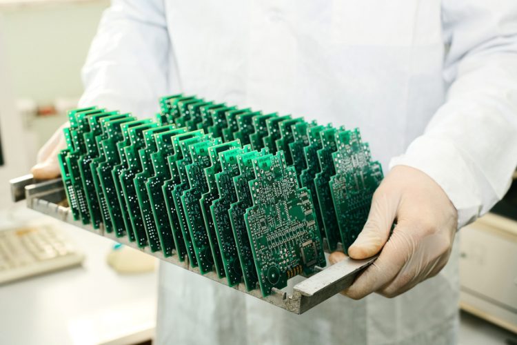
Printed Circuit Board (PCB) fabrication is the process of creating physical boards that electronically support and connect various components in electronic devices. PCBs are integral to the function of nearly all electronic devices, from simple gadgets to complex computer systems. Let’s get into it, shall we?
The PCB Fabrication Process
Design and Layout
The first step in pcb fabrication is designing the layout using specialized software like Eagle, Altium Designer, or KiCad. Designers create a schematic that outlines the electrical pathways and component placements. This layout is crucial as it ensures the PCB will function correctly when assembled.
Material Selection
PCBs are typically made from a non-conductive substrate, most commonly fiberglass, reinforced with epoxy resin. The conductive pathways are usually made of copper. The choice of materials affects the PCB’s durability, thermal stability, and performance.
Layering and Lamination
Modern PCBs often consist of multiple layers. These layers are laminated together using heat and pressure, ensuring they are properly aligned and bonded. The layers include the core substrate, copper layers, and insulating layers. Multilayer PCBs are used in complex devices requiring extensive circuitry.
Etching and Plating
After the layers are laminated, the next step is etching. This process involves removing excess copper to create the desired circuit pattern. In some cases, a chemical process is used, while other methods may include laser etching. Plating is then applied to the exposed copper to protect it and enhance conductivity.
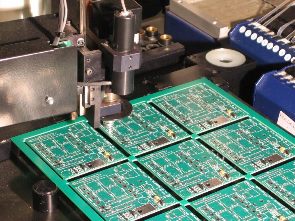
Drilling and Via Formation
Drilling precise holes, or vias, is critical for creating electrical connections between different layers of the PCB. These vias can be through-hole, blind, or buried, depending on the design requirements. Advanced techniques like laser drilling may be employed for high-precision needs.
Solder Mask and Silkscreen Application
A solder mask is applied to protect the copper circuits from oxidation and to prevent solder bridges during component assembly. The silkscreen layer adds labels and symbols on the PCB, aiding in the placement of components and providing information for assembly and troubleshooting.
Applications of PCBs
Consumer Electronics
PCBs are found in virtually all consumer electronics, including smartphones, laptops, televisions, and household appliances. They enable compact and efficient design, essential for modern electronic devices.
Medical Devices
In the medical field, PCBs are used in diagnostic equipment, imaging devices, and patient monitoring systems. High-reliability PCBs are critical for these applications to ensure patient safety and accurate results.
Industrial Equipment
Industrial machinery relies on PCBs for control systems, automation, and power management. Robust PCBs are essential for withstanding harsh industrial environments and ensuring long-term reliability.
Automotive and Aerospace
The automotive industry uses PCBs in engine control units, navigation systems, and safety features like airbags and anti-lock brakes. In aerospace, PCBs must meet stringent standards for performance and reliability, used in communication systems, control systems, and navigation equipment.
Conclusion
PCB fabrication is a sophisticated process that involves precise design, material selection, and intricate manufacturing techniques. The resulting PCBs are fundamental to the operation of countless electronic devices across various industries. As technology advances, the demand for more complex and reliable PCBs continues to grow, driving innovation in fabrication methods and materials.